Hybrid Perovksite
Starting with the “perovskite fever” in the field of photovoltaics, Hybrid Organic-inorganic Perovskite (HOP) materials have now become a key player in applications for optoelectronics, including solar cell, light emitting diode, laser and sensing. The Project Group “Perovskite” aims at developing novel perovskite optoelectronic devices in which light-matter interaction mechanisms are engineered in the subwavelength scale. This is achieved by structuring the HOP material into metasurface structures (see Fig.1). Functionalities and physical properties of perovskite devices will be implemented/enhanced by exploring innovative photonics concepts such as photon management, dispersion engineering, polaritonic physics at room temperature.

Fig. 1 : Top: Two technologies developed at INL to structure HOP layer into subwavelength-scale metasurface: (Left) Infiltration of HOP solution into photonic backbone, (Right) Thermal nano-imprint. Bottom: A perovskite solar cell fabricated at INL, with the HOP layer patterned in metasurface for light trapping.
Research Topics
Nanophotonic concepts for light management in perovskite solar cells
Perovskite has now become an alternative solution for silicon technology in the field of photovoltaics. Our distinctive approach is to implement nanophotonic concepts for boosting perovskite solar cell performance, while keeping its low-cost and solution-based fabrication process. As illustrated in Fig.2, the light management in perovskite solar cells results from three interdependent considerations: the photonic engineering at the wavelength scale, the material choices, and the nanofabrication processes. Practically, the last two directly define the solar cell architecture while the first one helps improving the way photons are “used” in the devices. Different photonic engineering strategies (anti-reflection, light-trapping, photon recycling, up-conversion) are combined to enhance energy conversion efficiency of single junction perovskite solar cell, tandem perovskite-silicon solar cell and even all-perovskite tandem solar cell [1].
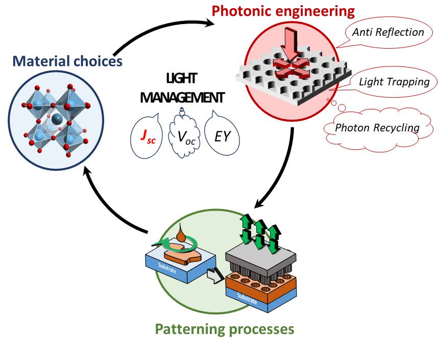
Fig. 2 : The three main correlated aspects that governed Light Management in perovskite solar cells. [1]
Perovskite-based polaritonic devices with excitonic metasurface
Exciton-polaritons are quasiparticles arising from the strong coupling regime between excitons in semiconductor and photons of resonant cavity. Polaritonic devices, inherited the best features of excitonic and photonic components, is a prominent platform to study fundamental physics of interacting bosons, as well as novel all-optical devices. Our original approach is to elaborate polaritons at room temperature by coupling 2D HOP excitons and Bloch photons of periodical metasurface (see Fig.3.a). In particular, both real part (i.e. energy) and imaginary part (i.e. losses) of polaritonic modes can be engineered via metasurface design. For the real part, polaritonic properties such as effective mass, group velocity and density of states can be tailored on-demand via energy-momentum dispersion engineering (Fig.3.b) [2]. For the imaginary counterpart, the radiative losses of HOP polaritonic mode can be suppressed using the concept of Bound State in the Continuum (BIC), resulting in a polarization vortex emission (see Fig.4) [3]. We also investigate the strong coupling regime between HOP excitons with peculiar photonic configurations (band inversion, exceptional points…) for perspective topological effects [4].
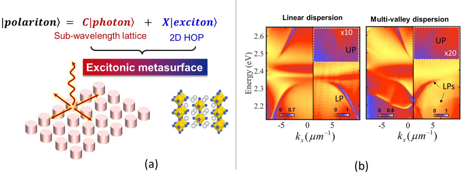
Fig.3. (a) Strong coupling regime in HOP-based excitonic metasurface. (b) Dispersion engineering of polaritonic modes in perovskite metasurface. Left panels are numerical simulations, right panels are experimental results. The strong coupling regimes are evidenced by the observation of avoid crossing effect. [2]

Fig.4. (a) Polarization vortex of polaritonic emission when coupling HOP excitons to photonic BIC in excitonic metasurface. (b) Experimental and (c) numerical simulation of polarization patterns of a polaritonic BIC in perovskite metasurface. [3]
Perovskite-based emitting devices
As direct band-gap semiconductor, perovskite material exhibit remarkable optical properties for emitting devices, such as tunable bandgap across the visible range, high luminescence quantum yield and narrow emission linewidth. In this topic, we study different original mechanisms to control the far-field emission of HOP-based light emitting diodes and micro-lasers (Figs.5 and 6): coupling perovskite thin-film to Bloch resonances [5], coupling perovskite quantum dots to photonic exceptional points [6], filtering perovskite random lasing via vertical cavity [7], …
Fig.5. Farfield emission of flat and patterned HOP layers [5].

Fig.6. Farfield emission of perovskite quantum dots when coupled to photonic exceptional points reveals the enhancement of local density of states at exceptional points. [6]
Projets
- Polaritonic devices based on hybrid perovskite in novel photonic crystal design – POPEYE (ANR JCJC funding)
- Electrically pumped hybrid perovskites based light-emitting devices – EMIPERO (ANR PRC funding)
- Métasuface excitonique à base de pérovskite pour dispositifs polaritoniques sur puce fonctionnant à température ambiante – PERSEPOLIS (IUF funding)
- Enhancement of Perovskite-based solar-cells and LEDs efficiency using plasmonic metamaterial – EPSILON (Pack Ambition International, La région Auvergne-Rhône-Alpes)
Group Members
- Coordinator: Hai Son Nguyen
- Permanent: Christian Seassal, Erwann Fourmond, Emmanuel Drouard, Céline Chevalier, Mohamed Amara, Sébastien Cueff
- PhD : Florian Berry, Nguyen Ha My Dang, Raphael Mermet Lyaudoz
References
[1] “ Light Management in Perovskite Photovoltaic Solar Cells: a perspective », Advanced Energy Materials (accepted), preprint: https://arxiv.org/pdf/2203.13891
[2] “Tailoring dispersion of room-temperature exciton-polaritons with perovskite-based subwavelength metasurfaces”, Nano Letters 20 (3), 2113-2119 (2020), preprint: https://arxiv.org/pdf/2001.06801
[3] “Realization of Polaritonic Topological Charge at Room Temperature Using Polariton Bound States in the Continuum from Perovskite Metasurface”, Advanced Optical Materials 2102386 (2022), preprint: https://arxiv.org/pdf/2110.15785
[4] “Engineering a light–matter strong coupling regime in perovskite-based plasmonic metasurface: quasi-bound state in the continuum and exceptional points”, Photonics Research 8 (12), A91-A100 (2020), open acess: https://doi.org/10.1364/PRJ.404743
[5] “Multiscale Simulation for Visible Light Communication using Perovskite Metasurface,” 2021 17th International Symposium on Wireless Communication Systems (ISWCS), 2021, pp. 1-6, preprint: https://hal.archives-ouvertes.fr/hal-03443483/document
[6] “Unveiling the Enhancement of Spontaneous Emission at Exceptional Points”, preprint: https://arxiv.org/pdf/2203.02245
[7] “Directing random lasing emission using cavity exciton-polaritons”, Optics Express 20 (3), 2113-2119 (2020), open acess: https://doi.org/10.1364/OE.410249

