Photonic crystal nanopattering of hybrid perovskite materials for photovoltaic solar cells and Light Emitting Diodes
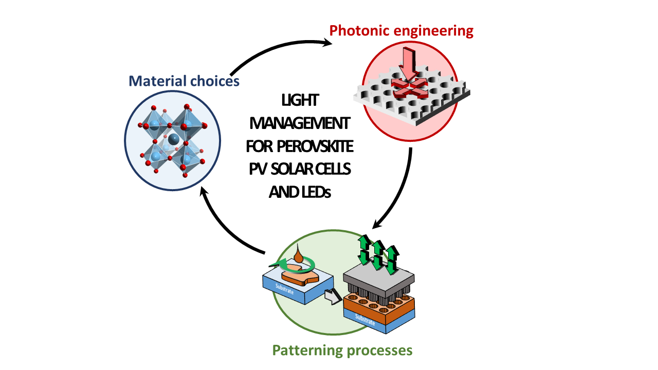
Together with in-depth understanding of the various materials, light management is essential for these perovskite solar cells to achieve their record performance. The i-LUM group at INL have a 15 year experience in the light management for thin films photovoltaics. Focus has been put on the direct patterning of the perovskite during the crystallization phase, developed at INL technological platform Nanolyon. Indeed, the resulting controlled nanopatterning, the so-called photonic crystal, is very well suited to drastically enhance the light-matter interaction.
Our group recently published a review paper in Advanced Energy Materials. In this paper, criteria on materials, processes, and photonic engineering are established to enhance primarily the short circuit current density for high energy yields. These criteria are used to analyze a large panel of solutions envisaged in the literature for single junction cells. It clearly appears that results in the literature using the approach we promote lead to the largest enhancements of the external quantum efficiency, especially close to the band-edge of the perovskite. In addition, a perspective is developed from rigorous electromagnetic simulations performed on various comparable structures. This also paves the way for further performance enhancement in the case of all-perovskite, two-terminal tandem cells.
Similar promising approach is also considered for enhanced efficiency and controlled radiation pattern of LEDs. To achieve, Nanolyon acquired in 2021 an industrial system, unique in a French laboratory: the NanoPatterning System NPS300, provided by SET corporation, that allows to obtain cm² samples using Nanoimprint Lithography in Step and Repeat mode. This still on-going work is done within the ANR project EMIPERO, coordinated by LUMin and associating XLIM and INL. All these laboratories are members of the GDR HPERO.
Contact: Emmanuel DROUARD
Reference: Berry, R. Mermet-Lyaudoz, J. M. Cuevas Davila, D. A. Djemmah, H. S. Nguyen, C. Seassal, E. Fourmond, C. Chevalier, M. Amara, and E. Drouard, “Light Management in Perovskite Photovoltaic Solar Cells: A Perspective,” Advanced Energy Materials 12, 2200505 (2022).