Nanowires and Nanostructures
Research activities
- Nanowire growth
At INL, we are investigating the growth mechanisms of semiconductor nanowires fabricated by molecular beam epitaxy using the vapor-liquid-solid method. With this procedure, it is possible to epitaxy axial or radial III-V semiconductor heterostructures (GaAs, GaP, InAs, InP). In order to finely control the structure and morphology of these nanowires, we have studied the physical chemistry of interfaces at the early stages of the growth using photoelectron spectroscopy [Fouquat 2019]. These nanowires have usually two different crystalline phases and the control of this parameter is a major challenge. In recent years, we have developed a strategy allowing us to control the nature of the crystalline phase. [Dursap 2020, Dursap 2021]. Obtaining GaAs nanowires in the wurtzite crystalline phase currently allows us to grow and study a particularly promising material: (Si) Ge in the hexagonal phase [Dudko 2021]. This semiconductor has a direct gap varying from 0.35 eV to 0.67 eV depending on the composition.
We are also actively developing the growth of heterogeneous core-shell nanowires [Guan 2016, Nscale & Guan 2016 NL]. This work presents both a fundamental interest, the study of a heterogeneous interface, and a practical interest, the functionalization of semiconductors to modify their (opto-)electronic properties.
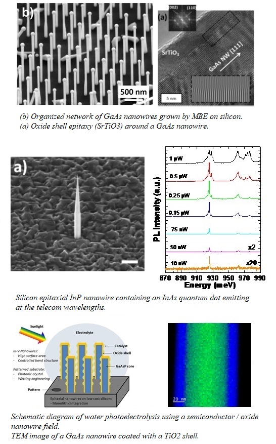
- Nanowires for ICT
III-V semiconductor nanowires have a particularly interesting geometry to integrate monolithically optical sources on silicon substrates. The main objective of this activity is the monolithic integration of bright single photon sources emitting in the telecom bands on silicon. We are specifically investigating InAs quantum dots embedded into InP nanowires produced by molecular beam epitaxy using the vapor-liquid-solid method [Jaffal 2020]. The carried out optical studies focus in particular in the measurements of the QD lifetime and emission intensity, the polarization state of the emitted photons and their radiation pattern [Jaffal 2019].
- Nanowires for renewable energies
This research activity aims to use III-V nanowires for the conversion of solar energy. Two approaches are currently investigated: the first consists of developing photovoltaic cells [Vettori 2019] in particular via “tandem” solutions to maximize yield, the second relies on photoelectrolysis of water for the generation of green hydrogen (ANR Beep project). This activity is interested in growth issues but also in the development of characterization techniques such as near-field or local probe microscopy to study the electronic properties at the scale of an individual nanowire.
Coordinators : N. Chauvin & J. Penuelas
Involved staff members : R. Bachelet, C. Botella, G. Brémond, N. Chauvin, A. Danescu, H. Dumont, J. Penuelas, P. Regreny, G. Saint-Girons
Current PhD students:
- Dursap (2018-2021) : « Nanofils III-V/oxyde pour la photoélectrolyse de l’eau »
- H.-G. Gloriès (2019-2022) : « Hétérostructures à base de nanofils III-V et d’oxydes fonctionnels pour les technologies de l’information »
- I. Dudko (2021-2024) : « Hexagonal Silicon and Germanium nanowires for light emission»
Former PhD students (last 5 years):
- Benali (2013-2017) : « Nanofils Ga(Al)As sur silicium pour le photovoltaïque de 3ème génération : simulation et croissance auto-catalysée »
- Mavel (2013-2017) : « Nanofils de semiconducteurs III-V épitaxiés sur Si(111) pour la photonique sur silicium »
- Becdelièvre (2014-2017) : « Etudes des propriétés électriques et mécaniques de nanofils GaAs : vers une modulation du transport par effet piézoélectrique ou ferroélectrique »
- Guan (2014-2017) : «Growth of semiconductor (core) / functional oxide (shell) nanowires : application to photoelectrochemical water splitting »
- Vettori (2015-2019) : « Growth optimization and characterization of regular arrays of GaAs/AlGaAs core/shell nanowires for tandem solar cells on silicon »
- Jaffal (2016-2019) : « InAs quantum dot in a needlelike tapered InP nanowire: a telecom band single photon source monolithically grown on silicon”
Scientific research fundings in progress:
– ANR PRC 2017-2023 : HEXSIGE
– ANR PRC 2018-2021 : BEEP
– EMPIR 2020-2023 : SRT-g013 NanoWires
– Labex iMUST 2022-2025 : HexaLight
Scientific research fundings (5 last years) :
– ANR PGER 2015-2019 : HETONAN
Collaborations :
C2N (Univ. Paris-Saclay), IEMN (Univ. Lille), IMEP-LAHC (Grenoble INP), Institut Camille Jordan (Univ. Lyon), LCBM (CEA Grenoble), LOMA (Univ. Bordeaux), LPS (Univ. Paris-Saclay), MATEIS (Univ. Lyon), SPEC (CEA Saclay), Synchrotron Soleil, Société SILSEF.