Chitosan : an abundant and natural polysaccharide
For the first time, a complete process of high resolution electron beam lithography and transfer by etching could be achieved from a natural, eco-friendly, positive tone and water- processable chitosan resist.
Currently, lithography uses oil based and hazardous chemicals as resists, solvents and toxic developers. These products are widely used in the classical micro- and nanofabrication techniques generating safety, waste management and related costs issues. Biosourced polymers can be used as an alternative for safer and more ecofriendly lithography. They are natural, abundant and, generally, water-processable, biocompatible and biodegradable. However, only few studies are undertaken on biopolymers in lithography. Generally, these studies do not bring a satifying answer since chemical modifications by syntheses are often required to functionalize biopolymers to enable their dissolution in a solvent or to enhance their reactivity under irradiation. Moreover, post-lithography patterning steps are not generally studied.
Among possible biopolymers, we have developped a bioresist based on chitosan, a hydrophilic polysaccharide prepared from chitin, the second most abundant biopolymer on Earth. This is a valorization product extracted from waste fish from food industry as crabs and shrimps shells [1]. Its solubility in aqueous solutions depends on pH. Thin films for mask patterning can be prepared from controlled chitosan aqueous solutions. It has a reactive ion etching resistance slightly higher than poly(methyl methacrylate) (PMMA), a synthetic organic polymer generally used for electron beam lithography.
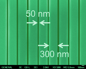
We have obtained extremely encouraging preliminary results. Our recent efforts have been focused on using the chitosan for sub-micron mask pattern transfer technique. We demonstrated that chitosan based positive resists using only water as solvent and developer were efficient for transferring accurately by reactive ion etching into silica hard mask underlying layer features of 50 nm [2] obtained by e-beam lithography (figure 1).
Légende :
SEM image of high resolution 50 nm lines spaced by 300 nm patterned into silica by electron beam lithography, water development and transfer by reactive ion etching from a chitosan resist
Contacts :
Yann CHEVOLOT, Jean-Louis LECLERCQ
Références :
[1] M. Rinaudo, “Chitin and chitosan : properties and applications”, Prog. Polym. Sci. 31, 603 (2006) ; https://doi.org/10.1016/j.progpolymsci.2006.06.001.
[2] M. Caillau et al., “50 nm lines patterned into silica using water developable chitosan bioresist and electron beam lithography”, Journal of Vacuum Science & Technology B, Nanotechnology and Microelectronics: Materials, Processing, Measurement, and Phenomena 35, 06GE01 (2017); https://doi.org/10.1116/1.4996870
Actualité scientifique CNRS – INSIS :
Des procédés de nanotechnologies plus écologiques grâce au chitosane