Structural and spectroscopic characterizations –modeling
Research themes
- Optical characterization
The team develops an expertise in both spatially-resolved and time-resolved optical spectroscopies to analyze at the nanoscale wires, particles and inclusions. The numerous experimental set-up allow optical studies from the UV to the mid-IR, from cryo temperature up to room temperature.
- Electrical characterization
The electrical and electronic spectroscopies of junctions, wires, particles, or inclusions, both at the nanometric scale and at the component scale, is a recognized expertise of the team. it relies in particular on the extensive use of electrical SPM (scanning probe microscopy) techniques.
- Structural and chemical characterization
The team has a large and versatile expertise harvesting X-ray diffraction, electron or ion diffraction, XPS/XPD, RBS and TEM/EELS. To those are added state-of-the-art techniques for structural analyses (surface diffraction, XPS-XPD, MEIS) and large facilities techniques in order to characterize and model the “structure-interface-stress” tryptic and solve the issue of heterogeneity in the studied materials or elaborated structures.
Our state-of-the-art knowledge in terms of thin film and micro-device characterization, associated with a constant improvement of our analysis techniques, allow applied studies linked to our industrial ecosystem. In particular, this knowledge is exemplified
- Stress engineering in thin films
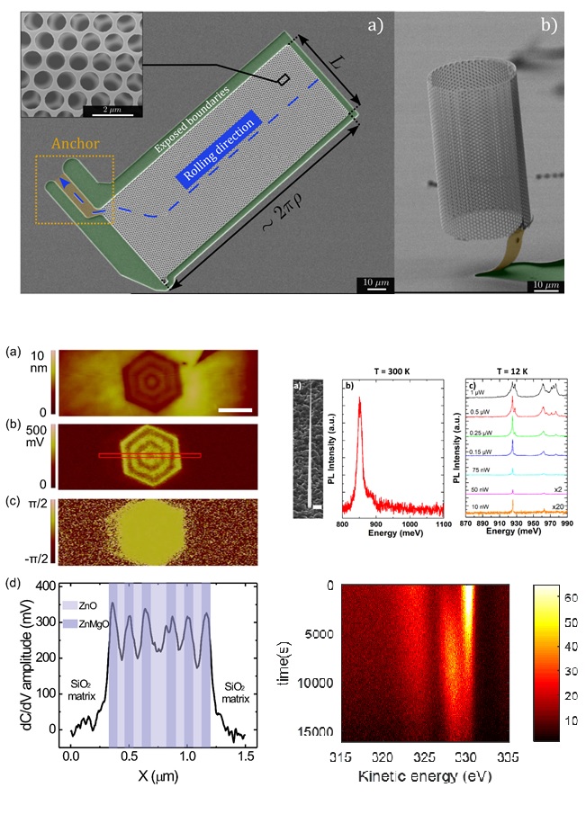
The control of the composition and thickness of epitaxial thin films allows the synthesis of tridimensional complex objects, by mechanical stress relaxation. In the framework of the ANR Pholding project, the implementation of this concept has led to the synthesis of wrapped photonic crystals, exhibiting remarkable optical properties (in term of light confinement).
Co-leaders of the thematic: G. Brémond and B. Masenelli
Members : A. Apostoluk, R. Bachelet, J.M. Bluet, C. Botella, G. Bremond, B. Canut, N. Chauvin,
A. Danescu, H. Dumont, C, Furgeaud, A. Lamirand, O. Marty, B. Masenelli, T. Nychyporuk, J. Penuelas,
P. Regreny, G. Saint Girons, B Vilquin, T. Wood
Ph-D students:
- Oleksander Synhaivsky (2017-2021) : « Propriétés électriques et piezoélectriques de nanofils de semiconducteurs à grands gaps ( ZnO) pour dispositifs hybrides »
- Younes Boussadi (CEA LETI) (2018-2021) : « Corrélation de mesures électro-optiques en température dans les micro-structures LED à puits quantiques InGaN/GaN pour applications micro-écrans »
- Thomas Nassiet (Cifre ST Microelectronics) (2018-2021) : « Technique innovante d’Imagerie de Photoluminescence : application aux technologies Imageur »
- Martina Zanetti (2020-2023) : « Microtechnologies génériques de décollement / report et recyclage du substrat pour fabriquer des dispositifs optoélectroniques : application aux imageurs infrarouges »
Former Ph-D students (last 5 years)
- Rémi Briche (2018-2021) : « Résonateurs photonique à base de Origami semi-conducteurs pour exalter l’interaction lumière/matière »
- Louise Fouquat (2015-2018) : « Etude par photoémission d’interfaces métal / oxyde et métal / semiconducteur élaborées par épitaxie par jets moléculaires »
- C. Zborowski (2014-2018): « Characterization of deeply buried interfaces by Hard X-ray Photoelectron Spectroscopy »
- Mariam El Khatib ( 2016-2019) « Etude et maîtrise des mécanismes de piégeage dans les composants MIS-HEMT en nitrure de gallium (GaN) pour la conversion de l’énergie « Etude
- Yu Zhang (CSC) (2016-2020) « Fabrication, structural and spectroscopic studies of wide bandgap semiconducting nanoparticles of ZnO for application as white light emitting diodes»
- Lin Wang (CSC) (2013-2016) «Carrier profiling of ZnO nanowire structures by scanning capacitance and scanning spreading resistance microscopy : Toward p-type ZnO ».
- Octavien Parredes-Saez (Cifre ST Microelectronics) (2014-2017) « Procédés d’épitaxie spécifiques au CMOS 14 et 10 nm: morphologie et structure ».
Post-doc:
Former Post-docs (5 last years):
- Ece Aybeke (2019-2020) « Mesures de dopage de nanofifls GaN et GaAs par SPM électrique » Projet région ENNORA
Projects:
– ANR ROLLER ( 2018- 2021)
– REGION ARA – ENNORA (2017-2022)
– ANR PHOLDING, 2017-2021
Former Projects (5 last years):
– ANR MaDFIZ ( 2013-2016)
Collaborations :
CEA LETI, C2P2 (Université Lyon 1), GEMAC (Université Versailles-St Quentin), LMGP (Université Grenoble Alpes), CEA LETI, ST Microelectronics, L2N (Université de Sherbrooke)