Tilting of ferroelectric domains by mechanical stress
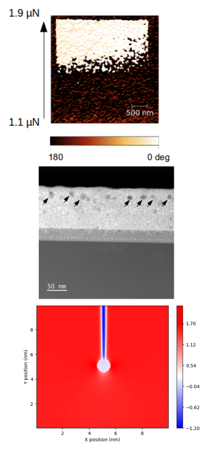
Ferroelectric materials are defined by the existence of a permanent dielectric polarisation at zero electric field, the direction of which can be switched by applying a sufficiently large electric field. We have shown that it is also possible to switch this polarisation by applying a mechanical stress to PbZr0.2Ti0.8O3 films with a thickness between 33 and 200 nm. The stress is applied by the tip of an atomic force microscope (AFM) and the polarisation reversal imaged by Piezoresponse Force Microscopy (PFM). The flexo-electric effect, which links the gradient of the mechanical stress to the electric field produced by the mechanical stress, cannot explain the polarisation reversal in such thick layers (only up to a few tens of nanometres thick). However, STEM-HAADF analysis revealed the existence of nano-cavities in the volume of the films which, combined with RBS analysis and phase-field simulations of the polarisation reversal, could explain the phenomenon: the cavities act as anchor points for the ferroelectric domains which can thus remain stable.
Contacts:
Ingrid C. Infante –
Damien Deleruyelle –
Brice Gautier –
Référence :
“Mechanical switching of ferroelectric domains in 33-200 nm thick sol-gel-grown PbZr0.2Ti0.8O3 films assisted by nanocavities”
Sergio Gonzalez Casal, Xiaofei Bai, Kevin Alhada Lahbabi, Bertrand Vilquin, Pedro Rojo-Romeo, Solène Brottet, David Albertini, Damien Deleruyelle, Matthieu Bugnet, Ingrid Canero-Infante, and Brice Gautier.
Advanced Electronic Material, 2022, 2200077, doi :10.1002/aelm.202200077